|
|
Rotates the object being placed/moved clockwise. Rotation is in increments of 90° |
||
|
|
Cycles through placement modes when placing a Wire/Bus/Signal Harness |
||
|
|
Changes the wiring mode for any connected wires, buses, or signal harnesses when dragging an electrical object |
||
|
|
Rotates the object being dragged clockwise. Rotation is in increments of 90° |
||
|
|
Copies attributes of the object currently under the cursor while placing an object of the same type |
||
|
|
Adds a vertex while placing a Wire, Line, Bus, Signal Harness, or Polygon |
||
|
+ |
On a selected segment of a placed Wire, Line, Bus, or Signal Harness or an edge of a placed Polygon to add a vertex at that point |
||
|
+ |
On a vertex of a placed Wire, Line, Bus, Signal Harness or Polygon to remove that vertex |
||
|
|
Cycle trhough the available vertex action modes (Deform, Scale, and Smooth) during sliding |
||
|
|
Remove the last placed segment, while placing a Wire, Line, Bus, Signal Harness, or Polygon |
||
|
ou
|
|||
|
|
Enlarges the size of the IEEE Symbol currently being placed/moved |
||
|
|
Reduces the size of the IEEE Symbol currently being placed/moved |
||
|
|
On a net object, to highlight all objects associated to that net across all sheets of the active design project |
||
|
|
On a Sheet Entry to jump to the corresponding port on the sub-sheet referenced by that entry's parent Sheet Symbol |
||
|
|
On a Port to jump to the corresponding sheet entry in the parent sheet symbol that references the sub-sheet on which the port resides |
||
|
|
On a port to jump to another port with the same name, on the indicated target schematic document (only available when the Net Identifier Scope - set on the Options tab of the Project Options dialog - is set to Flat, or Global) |
||
|
|
On a sheet symbol to descend the design hierarchy to open the child sheet referenced by that symbol |
||
|
|
Relocate the currently selected Sheet Entry (or entries) that are being moved, to the directly opposite side of the parent Sheet Symbol |
||
|
|
Reverse order while moving two or more selected Sheet Entries |
||
|
|
Toggle IO Type while moving one or more selected Sheet Entries |
||
|
|
Toggle IO Type for all Sheet Entries while graphically resizing the parent Sheet Symbol |
||
|
Sub menu shortcuts
|
|||
|
|
Align sub-menu |
||
|
|
Toolbars sub-menu |
||
|
|
Jump sub-menu |
||
|
|
Panels sub-menu |
||
|
|
Move sub-menu |
||
|
|
Right-click Options sub-menu |
||
|
|
Select sub-menu |
||
|
|
DeSelect sub-menu |
||
|
|
Right-click Filter sub-menu |
||
|
|
Pop-up menu with zoom commands |
||
Publicité
|
|
With an initial object selected in the design, extend the selection to include the next higher-level object (or objects), based on logical hierarchy. In addition, the feature caters for selection extension across multiple objects selected across different nets in the design. |
||
|
|
Single select the next design object in a set of co-located (overlapping) objects without utilizing a selection pop-up window. To use this command, ensure that the Display popup selection dialog option is disabled on the PCB Editor - General page of the Preferences dialog. |
||
|
|
Enable Cross Select Mode |
||
|
|
Select all objects on the current document |
||
|
|
Select all objects that reside within the boundary of the defined board shape |
||
|
|
Select all electrical objects that are connected to the same piece of copper |
||
|
|
Copy selected object(s) and paste repeatedly where needed in the workspace (rubber stamping) |
||
|
|
Paste objects onto the current layer regardless of their original layer assignments |
||
|
|
Align selected objects by their left edges |
||
|
|
Align selected objects by their right edges |
||
|
|
Align selected design objects by their left edges while maintaining adequate spacing in observance with applicable design rules |
||
|
|
Align selected design objects by their right edges while maintaining adequate spacing in observance with applicable design rules |
||
|
|
Make the horizontal spacing of selected objects equal |
||
|
|
Align selected objects by their top edges |
||
|
|
Align selected objects by their bottom edges |
||
|
|
Align selected design objects by their top edges while maintaining adequate spacing in observance with applicable design rules |
||
|
|
Align selected design objects by their bottom edges while maintaining adequate spacing in observance with applicable design rules |
||
|
|
Make the vertical spacing of selected objects equal |
||
|
|
Move selected components to the nearest point on the required component placement grid |
||
|
|
Move the cursor to the absolute origin at the lower-left corner of the workspace |
||
|
|
Move the cursor to the relative origin of the current document (PCB document), or the location of the component reference point (PCB Library document) |
||
|
|
In the workspace to access the Selection Memory dialog, from where you can control all aspects of the selection memory feature |
||
|
|
In a dialog or panel to toggle the measurement units (in the dialog or panel only), between metric (mm) and imperial (mil) |
||
|
|
… to |
||
|
|
… to |
||
Publicité |
|||
|
|
… to |
||
|
|
… to |
||
|
|
… to |
||
|
|
ActiveRoute selected connections |
||
|
|
Access the Find Similar Objects feature (click on an object to use as the base template) |
||
|
|
Switch the display of the PCB workspace to Board Planning Mode |
||
|
|
Switch the display of the PCB workspace to 2D Layout Mode |
||
|
|
Switch the display of the PCB workspace to 3D Layout Mode |
||
|
|
Switch the display of the PCB workspace to 2D Layout Mode and see the same location and orientation of the board as you switch. |
||
|
|
Switch the display of the PCB workspace to 3D Layout Mode and see the same location and orientation of the board as you switch. |
||
|
|
Display all design objects on the current document |
||
|
|
Zoom-in, relative to the current cursor location |
||
|
ou
|
|||
|
|
(then move the mouse forward) Zoom-in, relative to the current cursor location |
||
| ou + | |||
|
(click and hold the mouse wheel, then move the mouse forward) Zoom-in, relative to the current cursor location |
|||
|
|
Zoom-out, relative to the current cursor location. |
||
|
|
Zoom-out, relative to the current cursor location |
||
|
|
(then move the mouse forward) Zoom-out, relative to the current cursor location |
||
| ou + | |||
|
(click and hold the mouse wheel, then move the mouse forward) Zoom-out, relative to the current cursor location |
|||
|
|
Zoom-in, relative to the current cursor location and in progressively smaller steps |
||
|
|
Zoom-out, relative to the current cursor location and in progressively larger steps |
||
|
|
Set the magnification of the current document to 400% |
||
|
Scroll vertically within the design workspace. This is a default setting that can be changed from the System - Mouse Wheel Configuration page of the Preferences dialog |
|||
|
|
Scroll horizontally within the design workspace. This is a default setting that can be changed from the System - Mouse Wheel Configuration page of the Preferences dialog |
||
|
|
Redraw the view in the main design window, placing the location marked by the cursor - prior to launching the command - at the center of the window |
||
|
|
Refresh the screen, in effect performing a redraw of the current document, to remove any undesirable drawing update effects |
||
|
|
Jump to, and make active, the previous component in the current library document. After reaching the first component in the list, the command will not cycle to the last component again. |
||
|
|
Jump to, and make active, the next component in the current library document. After reaching the last component in the list, the command will not cycle to the first component again |
||
|
|
Redraw the current layer of the current document, to remove any undesirable drawing update effects |
||
|
|
Toggle the display of the current document's editor between maximized and not maximized |
||
|
|
Visually toggle the Net Color Override feature on or off |
||
|
|
Toggle the Heads Up Display on or off |
||
|
|
Toggle Heads Up Display tracking on or off |
||
|
|
Resets the Delta Origin point for the Heads Up Display feature to 0,0 |
||
|
|
Toggle the 3D model visibility in the current PCB document |
||
|
|
Toggle the display of the Delta coordinates within the Heads Up Display |
||
|
|
Cycle to the next mode of object Hotspot Snapping |
||
|
|
Access the dedicated grid editor dialog for the snap grid currently under the cursor |
||
|
|
Set the X (horizontal) and Y (vertical) step values - for the default Global Board Snap Grid - simultaneously to a chosen value |
||
|
|
Temporarily disables the grid |
||
|
|
Toggle on/off whether the cursor on a grid will snap to the active workspace grid. Once enabled, the cursor will pull or snap to the nearest snap group location |
||
|
|
Toggle the measurement units for the current document between metric (mm) and imperial (mil) |
||
|
|
Toggle the display of the Difference Map Overlay in the main design workspace On or Off |
||
|
Note: This command is available only provided a comparison has been performed from the Collaborate, Compare and Merge panel.
|
|||
|
|
Toggle the state of the current cell containing detected differences between checked and unchecked when using Altium Designer's Collaborative PCB Design functionality |
||
|
|
Navigate to the previous cell containing one or more detected differences when using Altium Designer's Collaborative PCB Design functionality |
||
|
|
Navigate to the next cell containing one or more detected differences when using Altium Designer's Collaborative PCB Design functionality |
||
|
|
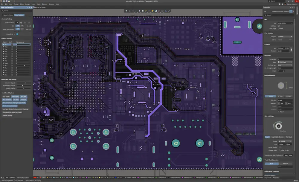
Access the Layers And Colors tab of the View Configuration panel in which you can configure the display of layers for the board and the colors assigned to those layers |
||
|
|
Access the View Options tab of the View Configuration panel in which you can configure the mode used to display each of the various design items within the workspace |
||
|
|
Access the Board Insight pop-up, listing all violations (of defined Design Rules) currently under the cursor |
||
|
|
Access the Board Insight pop-up, listing all components and/or net objects currently under the cursor |
||
|
|
Measure and display the distance between any two points in the current document |
||
|
|
Move the cursor to the left in the current document workspace in increments of one snap grid unit |
||
|
|
Move the cursor to the left in the current document workspace in increments of 10 snap grid units |
||
|
|
Move the cursor to the right in the current document workspace in increments of one snap grid unit |
||
|
|
Move the cursor to the right in the current document workspace, in increments of 10 snap grid units |
||
|
|
Move the cursor upwards in the current document workspace, in increments of one snap grid unit |
||
|
|
Move the cursor upwards in the current document workspace, in increments of 10 snap grid units |
||
|
|
Move the cursor downwards in the current document workspace, in increments of one snap grid unit |
||
|
|
Move the cursor downwards in the current document workspace, in increments of 10 snap grid units |
||
|
|
Move the current selection (one or more selected design objects) to the left in the current document workspace in increments of one snap grid unit |
||
|
|
Move the current selection (one or more selected design objects) to the left in the current document workspace, in increments of 10 snap grid units |
||
|
|
Move the current selection (one or more selected design objects) to the right in the current document workspace, in increments of one snap grid unit |
||
|
|
Move the current selection (one or more selected design objects) to the right in the current document workspace, in increments of 10 snap grid units |
||
|
|
Move the current selection (one or more selected design objects) upwards in the current document workspace, in increments of one snap grid unit |
||
|
|
Move the current selection (one or more selected design objects) upwards in the current document workspace, in increments of 10 snap grid units |
||
|
|
Move the current selection (one or more selected design objects) downwards in the current document workspace, in increments of one snap grid unit |
||
|
|
Move the current selection (one or more selected design objects) downwards in the current document workspace, in increments of 10 snap grid units |
||
|
|
Change the selection status of the object currently under the cursor without affecting the status of other objects |
||
|
Select/deselect the object currently under the cursor |
|||
|
|
On a net object to highlight the entire routed net |
||
|
|
On a layer tab to highlight all content on that layer |
||
|
|
In free space to clear current highlighting |
||
|
|
On a net object to highlight the entire routed net in addition to the routed nets already highlighted (cumulative routed net highlighting) |
||
|
|
On a layer tab to highlight all content on that layer in addition to the content already highlighted on other layers (cumulative layer highlighting) |
||
|
|
On a connection to select that connection |
||
|
|
On a connection to select that connection in addition to the connections already selected (cumulative connection selection) |
||
|
|
(drag from right to left) To select all connections touched by the dragged rectangle |
||
|
|
While hovering the cursor over a layer tab to highlight the content of that layer only |
||
|
|
(hold) Create a vertex (or break) in a track segment at the current cursor position |
||
|
Modify the properties of the object currently under the cursor |
|||
| + |
(click an object, hold and drag) Move the single object currently under the cursor (or group of selected objects if the object is part of that selection) |
||
|
(click an object, drag from left-to-right) Select all objects that fall completely within the bounds of the selection area |
|||
|
(click an object, drag from right to left) Select all objects that fall completely inside the selection area or are touched by its boundary |
|||
| + |
Display the slider (panning) hand cursor then drag to move your view of the workspace |
||
|
Access context menu for workspace or object currently under the cursor. If currently within an interactive command, will escape from the current operation |
|||
|
|
Toggle the display of the Properties panel accordingly |
||
|
|
Toggle the display of the PCB Filter panel or the PCBLIB Filter panel accordingly |
||
|
|
Toggle the display of the PCB List panel or the PCBLIB List panel accordingly |
||

Quel est votre raccourci clavier préféré Altium Designer Avez-vous des conseils utiles pour le programme ? Faire savoir aux autres.
1058833 62
477900 4
397319 18
329794 4
281615
261621 3
Il y a 6 heures
Il y a 3 jours Mis à jour !
Il y a 3 jours Mis à jour !
Il y a 4 jours
Il y a 6 jours
Il y a 7 jours
En son yazılar